Products for PCB’s industry
Preparation of copper surfaces for PCB industry
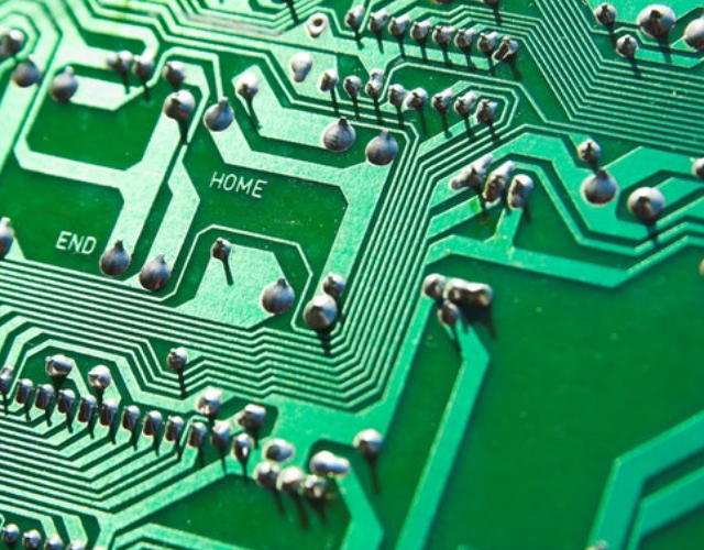
NTS offers two product lines suitable for the preparation of the copper surfaces for improving the adhesion of photoresists and soldermasks for the production of printed circuit boards.
> Before photoresist for inner and outer layers
> Before photoresist for inner and outer layers, and soldermask
The strengths of products microetching :
- Regularity and uniformity of copper microetching
- Chemical stability
- Quality of copper preparation in the case of PCBs with blind holes and buried holes
- Preserve the thickness of copper in the holes
- Economic use
- Easy treatment of rinse water
Preparation of copper surfaces before photoresist for inner and external layers of PCB
Circuit boards with high definition fine line, with copper tracks often below 100 microns wide, requires very good surface preparation of copper.
The contact must be perfect between the resist and the copper surface of the PCB.
For this reason the mechanical brushing, sanding, scrub, etc … are not sufficiently effective.
This is why NTS has created the formula of ETCHBRITE, product-based sulfuric acid and stabilized hydrogen peroxide, For the preparation of copper surfaces during the manufacture of printed circuits.
The ETCHBRITE 5XXX is an acid formula, degreasing, microetching copper for preparation before coating soldermask, for inner and outer layers before resist and other applications such as HAL.
The ETCHBRITE 5XX dissolved 40 g / l of copper by attacking at a constant speed and uniform.
The ETCHBRITE contains non-foaming surfactants that remove fingerprints and traces of fat. After drying the copper remains passivated which prevents it from oxidizing.
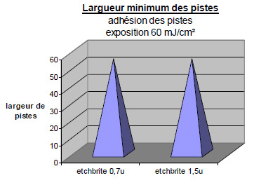
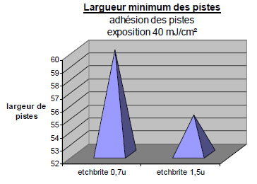
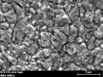
Examples of microetching NTS 519
Microetching for the preparation of copper for inner layers and outer layers of the printed circuits
Copper processed in fabrication with NTS519
X5000
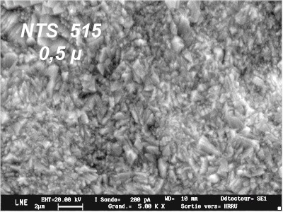
Examples of microetching NTS 515
Microetching inner layers
Copper processed in fabrication with NTS515
X5000

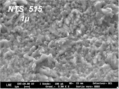
Microetching electrolytic copper
Copper processed in fabrication
X5000
Preparation of copper surfaces before photoresist for inner and outer layers, and soldermask
Micro-Etch Adherence promoter
Micro-Etch NTS 535 has been formulated to solve the adhesion problems of soldermask in the case of surface finishing such as nickel / gold and immersion tin.
Micro-Etch NTS 535 is an acidic solution, stable, ready to use.
Micro-Etch NTS 535 is economical, it dissolves 55 g / l of copper and is easily controlled by analysis according to the treated surface or by colorimetry.
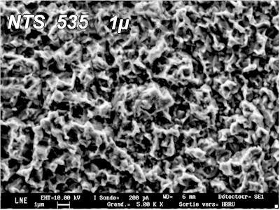
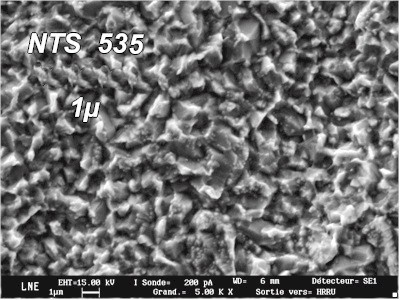
Examples of microetching NTS 535
Microetching copper inner layers
Copper processed for the manufacture of printed circuits NTS535
X5000
Microetching electrolytic copper
Copper processed for the manufacture of printed circuits NTS535
X5000
